Make a PCB from scratch using EasyEDA // Part 2 // Tutorial
This is the second part of my video on building a simple PCB using EasyEDA.
In this video we’ll be taking a look at how to use a solder stencil, placing SMD components, soldering using kitchen equipment and how to fix up your mistakes.
Intro
If you watched Part 1 of this video you would have seen me design a simple PCB using EasyEDA. This board I’ll soon be selling on Tindie. So unlike my mmBoard, which was a total April Fool’s joke, this one is for real.
Building boards by hand is a very time consuming task. If you have more than 4 boards to make and have access to a Pick & Place machine, then that way will be a lot faster.However, since I’m only building four boards, it’s faster to do it by hand.
So, the package arrived pretty quickly. In fact I placed the order on a Friday and the package arrived on Monday afternoon. Of course, EasyEDA knew who I was but my take on it is; if they can do it once they can do it again.
I didn’t find any issues at all with the PCBs and was pretty impressed with the accuracy of the silk screen printing. If you check out EEVBlog forums they say pretty much the same thing.
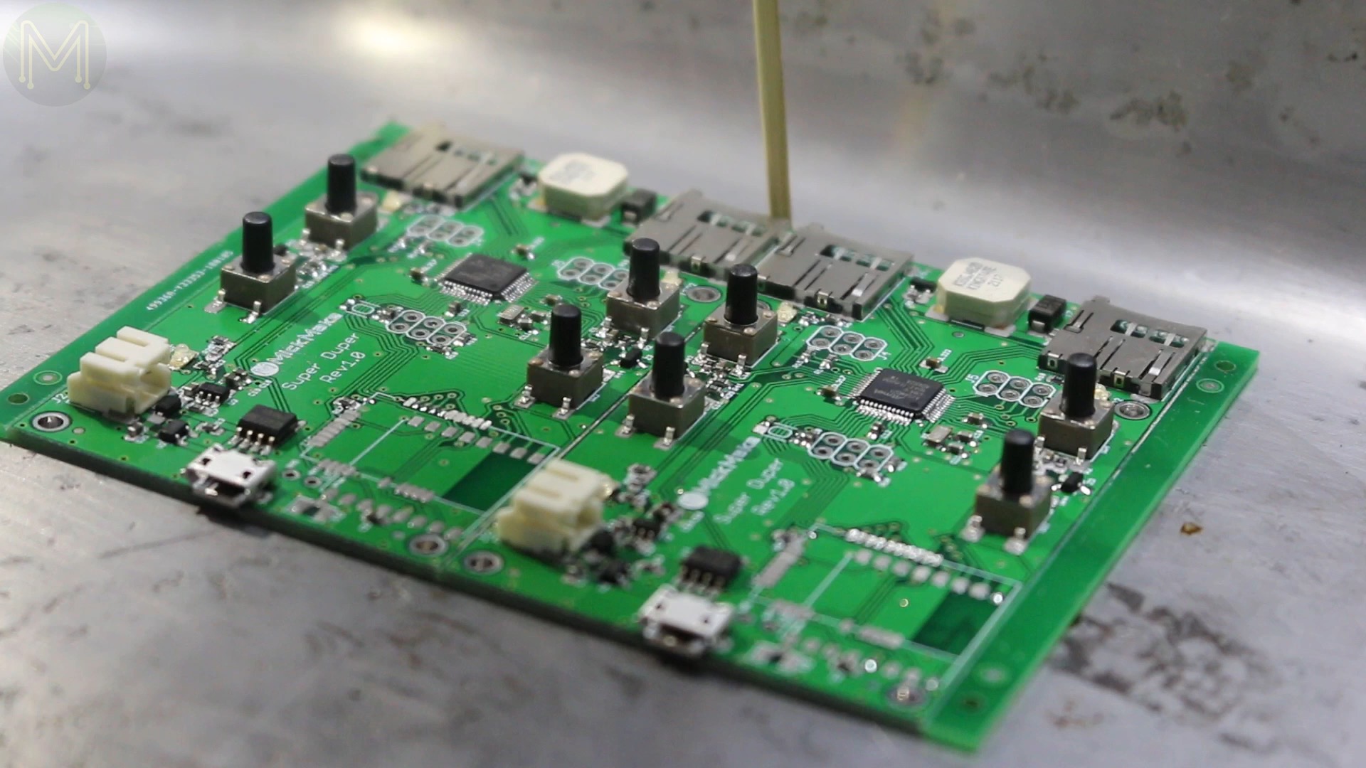
With this batch of PCBs, I ordered 10x panelized PCBs.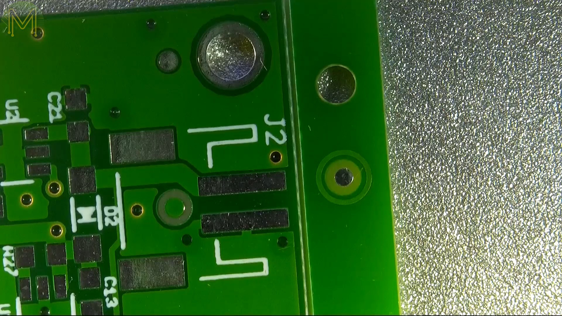
Paneling is a way of getting more for the same cost. The reason for this is, you will pay the same cost for any board size up to 100mm by 100mm. So if your board is say 40mm by 40mm, then placing 4 boards within that area won’t cost you any more.
It also makes Pick & Place a lot quicker as you would be building 4 boards at once. EasyEDA offer a free paneling service, so you just select the layout and you’re good to go.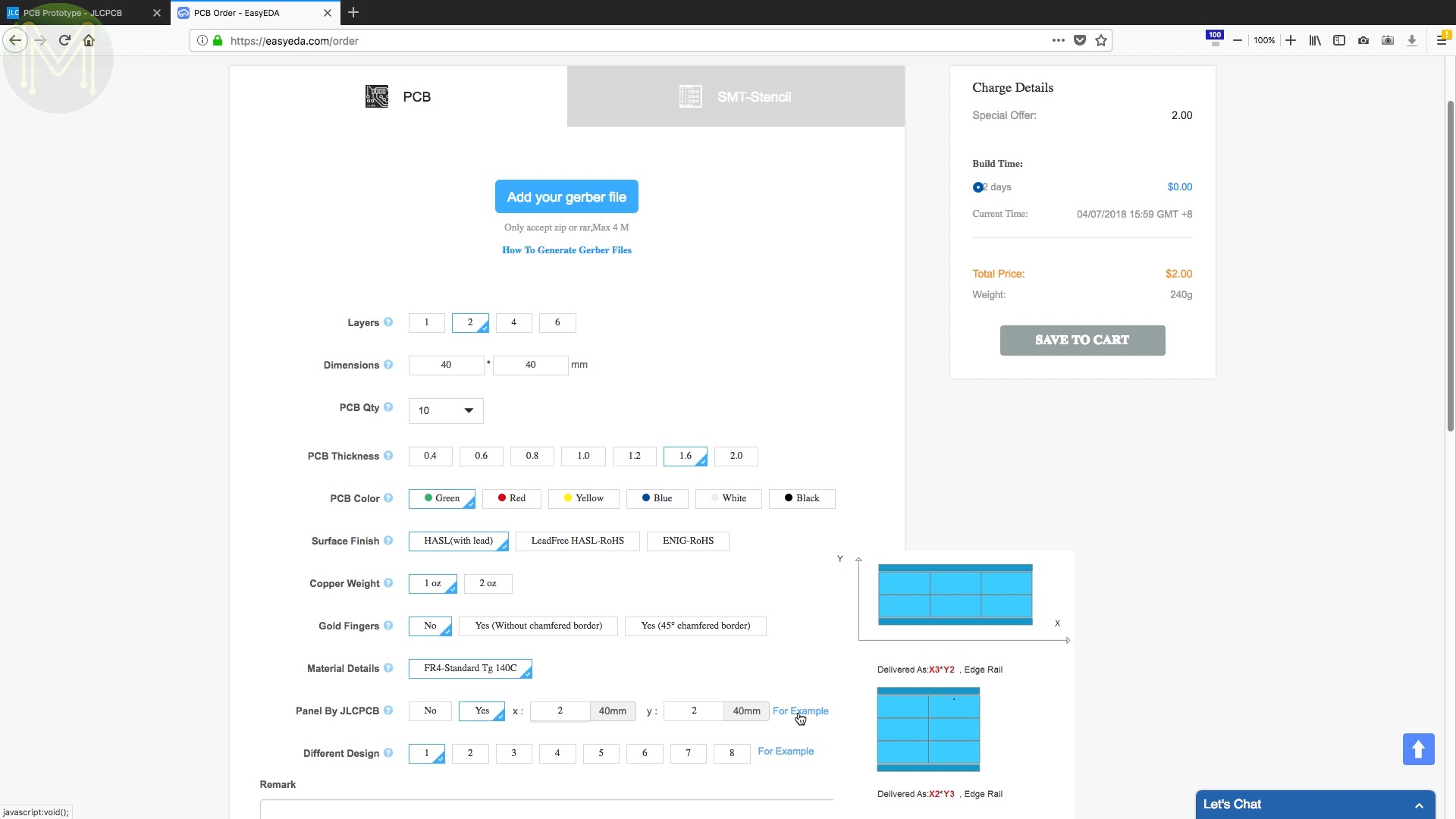
I also ordered a stencil. This costs extra, but as you’ll see in this video, if you’re doing a number of boards you really can’t do without it.
So, let’s get stuck into building the boards by hand.
Preparation
To build the boards, you’ll, of course, need all the parts available. You’ll also need a list of parts, bunched and sorted by package height. You want to be able to place the smaller components first, otherwise you risk bumping things.
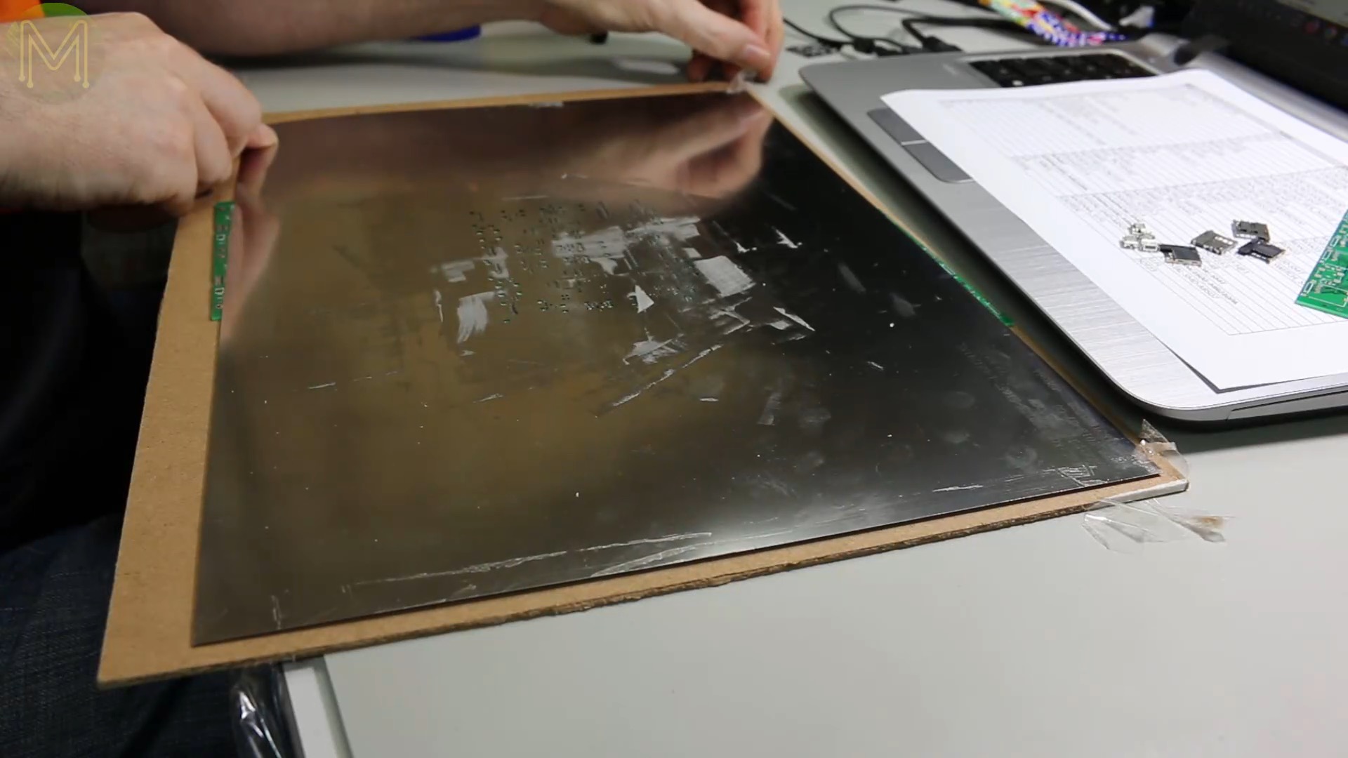
Next crack out the stencil. The stencil is used to apply a very thin layer of solder paste to the PCB.
First you need to carefully remove it from the backing plate. I ordered an un-framed stencil. If you order a frame around it, it’ll cost more, but is sturdier.
You need to treat these stencils very carefully. If you have any bend in them, they will be effectively useless.
So several rules when using stencils: 1. Treat them like they are made of tissue paper. 2. Always keep them clean before and after use - you can use isopropynol for this. 3. When not in use, keep them secure in the backing. 4. Did I mention to always keep them clean?
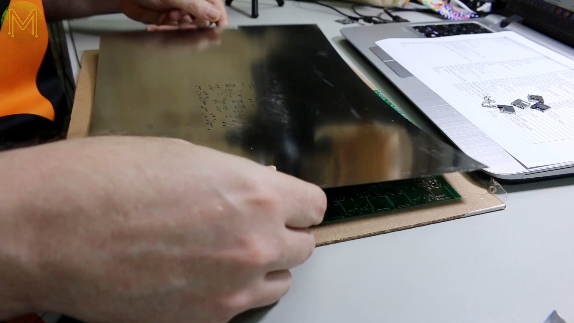
Once you have your stencil cleaned up, you’ll need to stick down some holders that hold the PCB in place.Remember you’re dealing with fractions of a mm here. So, it needs to be secure. Also make sure that the PCB is stuck down, otherwise it might lift up when you remove the stencil.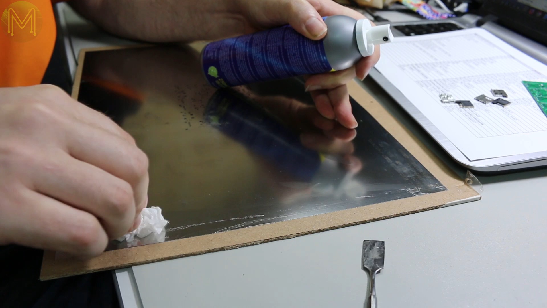
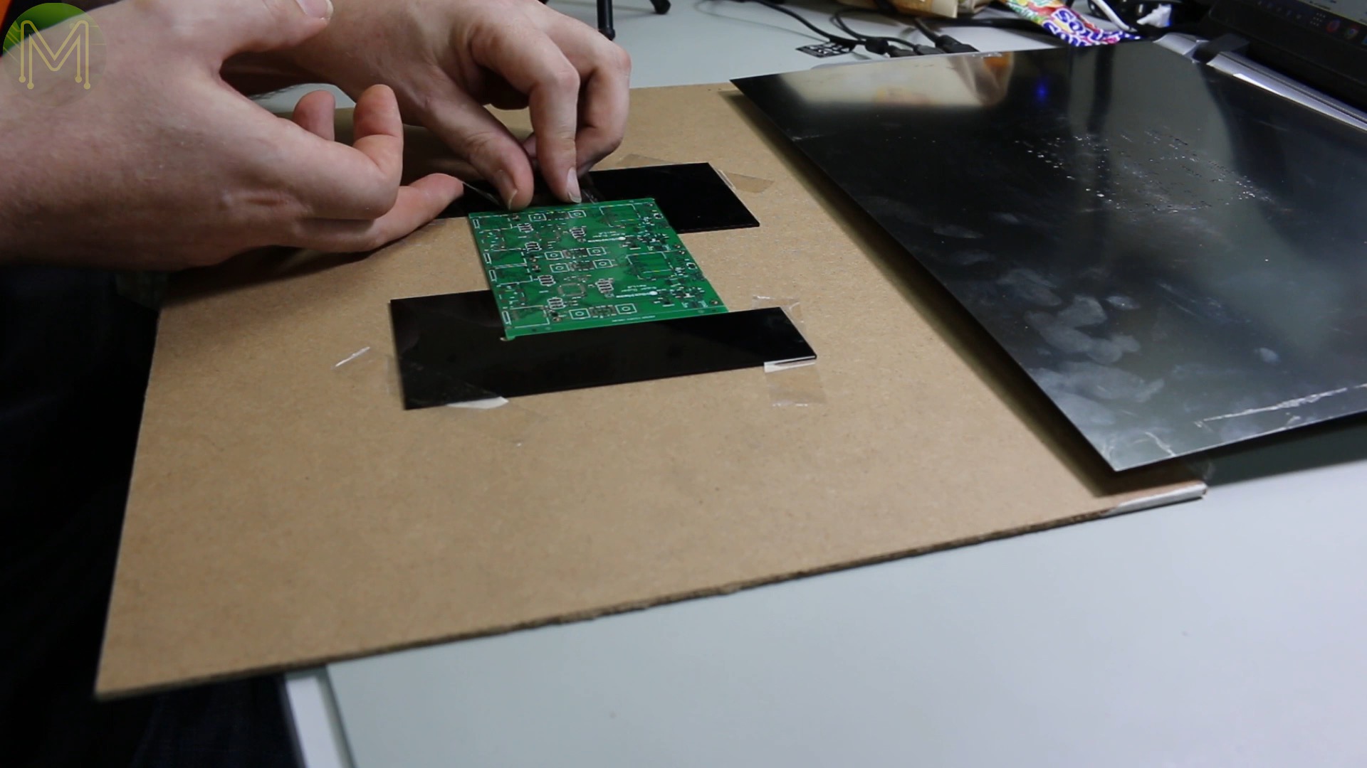
Next arrange a bunch of spare PCBs around the place. This avoids the stencil warping when you press down on it.
Then spend some time lining up the stencil with the pads. The easiest way is to pick the largest hole first and roughly line things up. Then pick a smaller package, ideally an MCU, to fine tune it.Next tape down the corners securely. You don’t want that thing moving one fraction of a mm.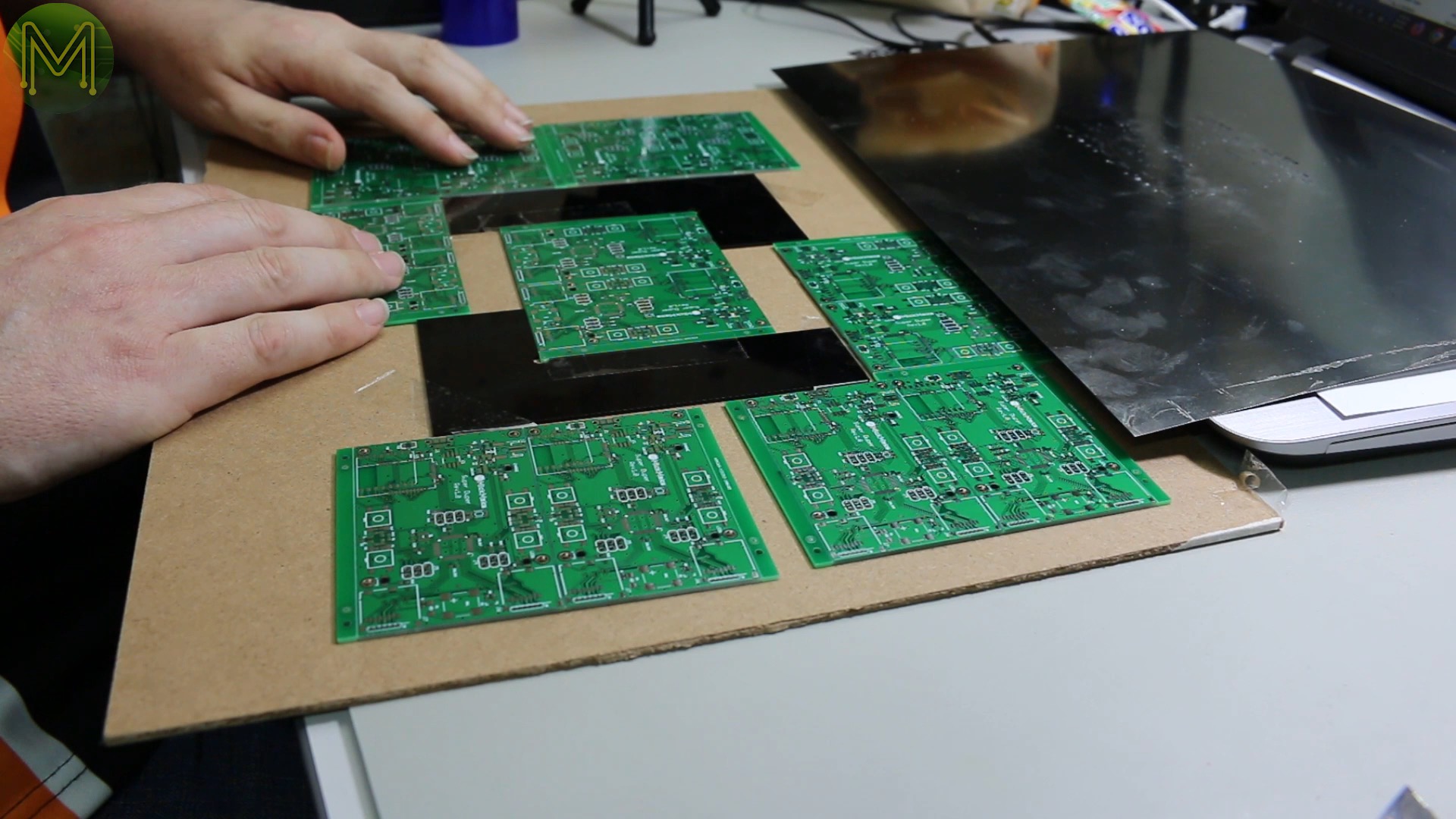

Applying solder paste
Next is the messy bit. Of course, you’ll need some solder paste. I used this solder paste, which is a lead-free variant.
It basically means that you won’t kill yourself slowly with lead poisoning, which is always a good thing. The other good thing about this solder paste is that it can stay on the boards for up to 8 hours without drying up. That’s plenty of time to get these boards loaded and soldered.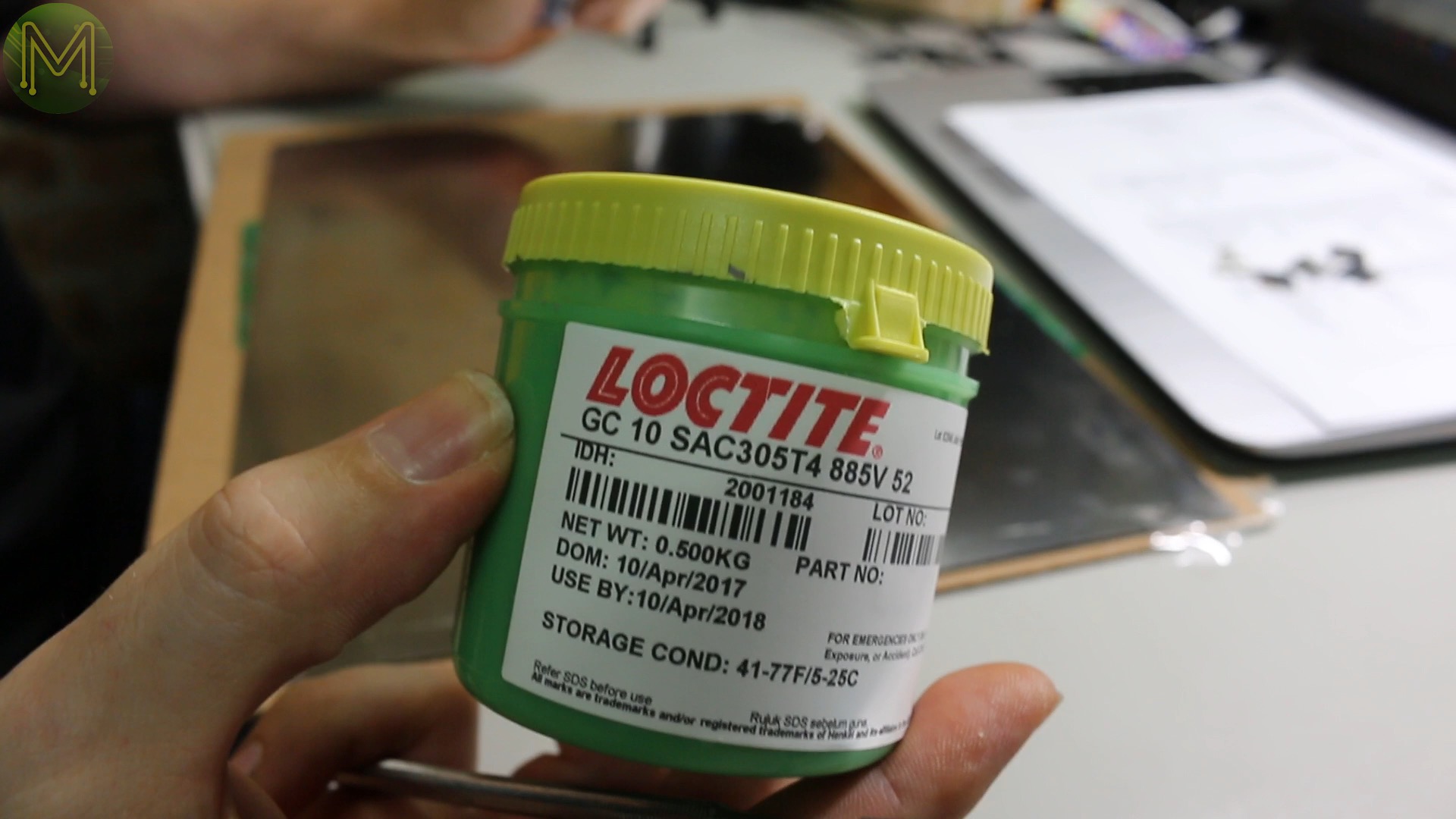
The process is pretty simple. Apply solder paste to the edge of a card so that you have a nice even line.
Credit cards work well as they are ridged with a bit of flexibility, but you really should use a card that is bigger than the PCB and only make one pass over the board.The reason for this is that the stencil doesn’t really lie completely flat.When you apply solder paste the stencil can move up slightly as you pass over. As it moves up, it can produce a small vacuum that sucks solder back on to the board.When you pass over it again, the stencil pushes that bit down onto the PCB. The problem gets worse, the passes you make. And once you have solder paste underneath the stencil, things go from bad to worse and you’ll have to just stop, clean both the PCB and stencil, and start again.Next you’ll need to remove the stencil very carefully. Any slight movement and you’ll mess up the solder.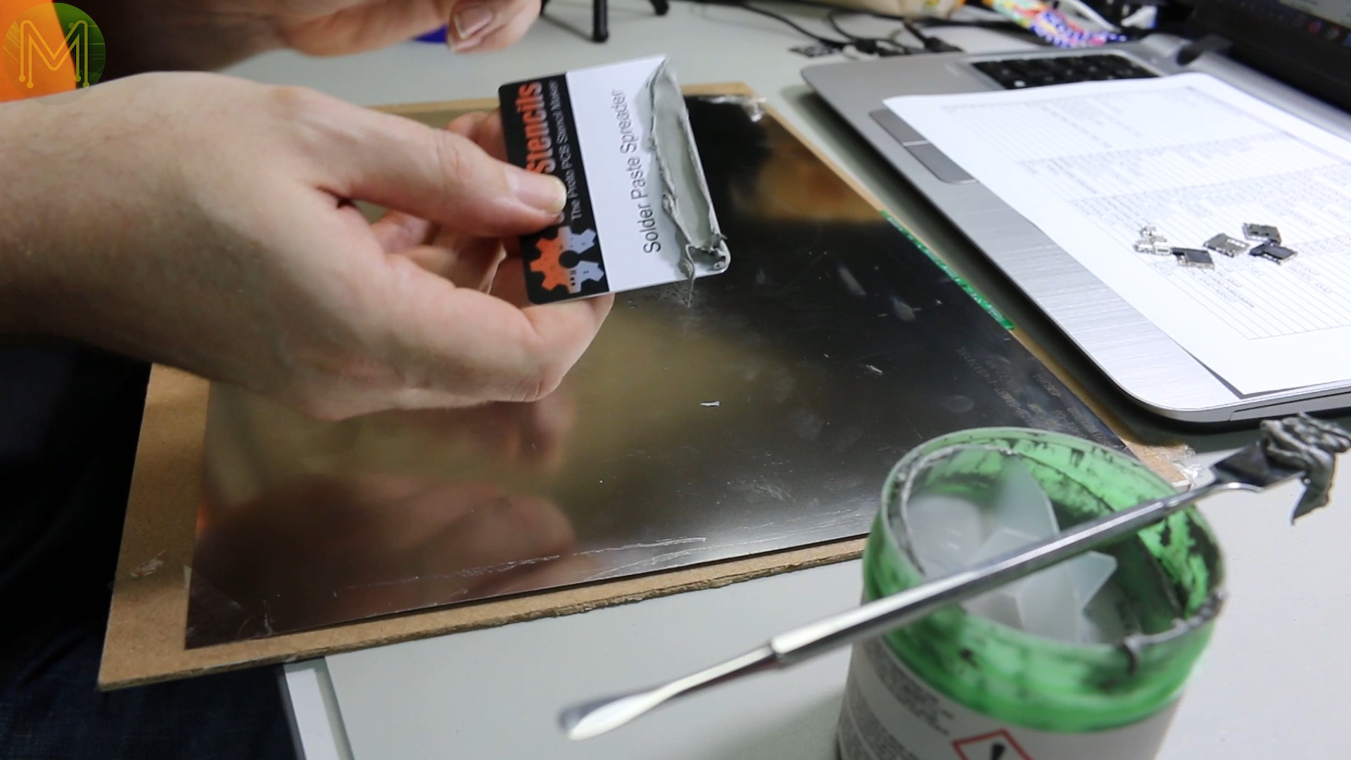
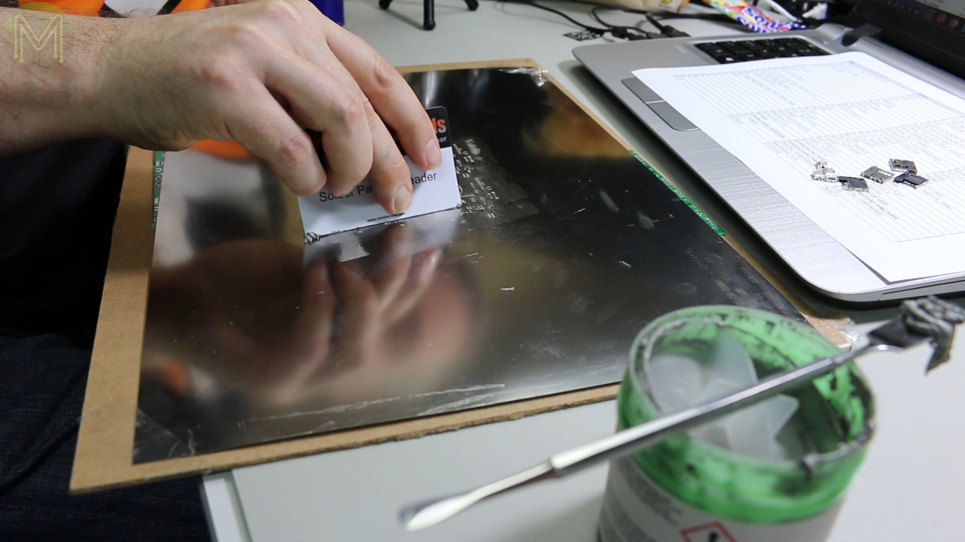

For example; the second batch of boards I moved the stencil very slightly. It completely stuffed everything up.
If you do this, you’ll need to thoroughly clean both the PCB and stencil, and start again.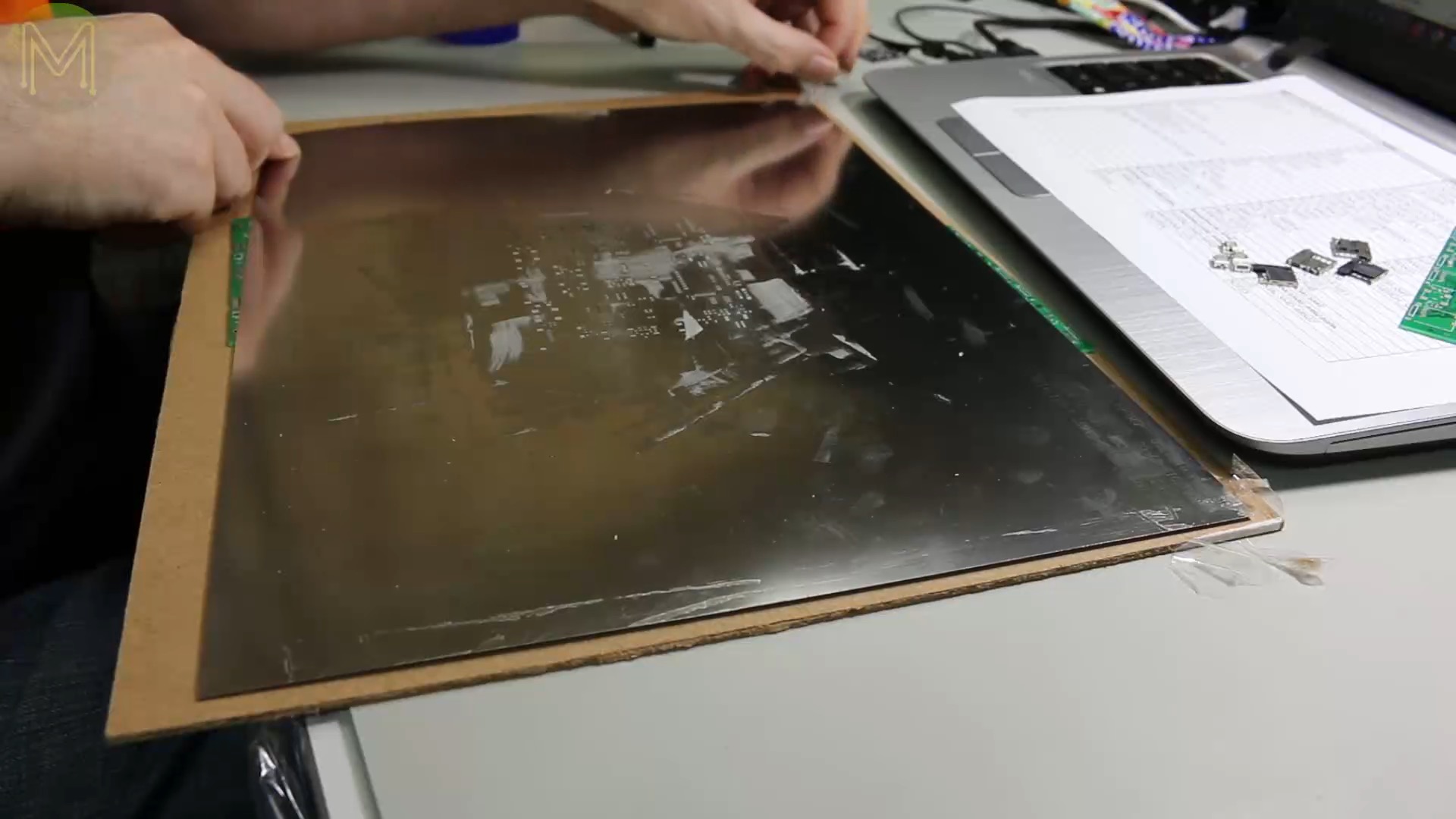
After you’ve removed the stencil, visually inspect to make sure everything is OK.
Then cleanup. Pack away any spare solder back into the container. Set aside the PCBs you’ve pasted and cleanup the stencil. You don’t want any dry solder paste stuffing things up later.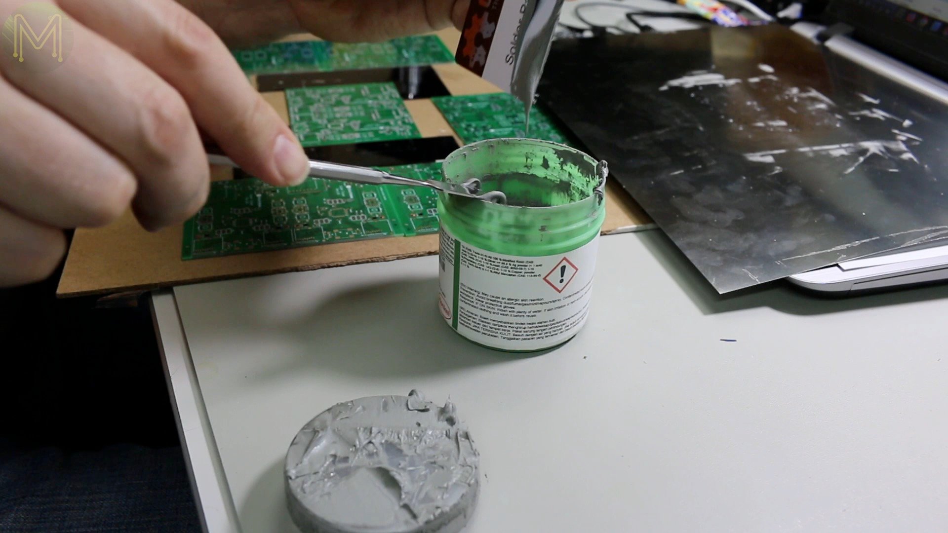
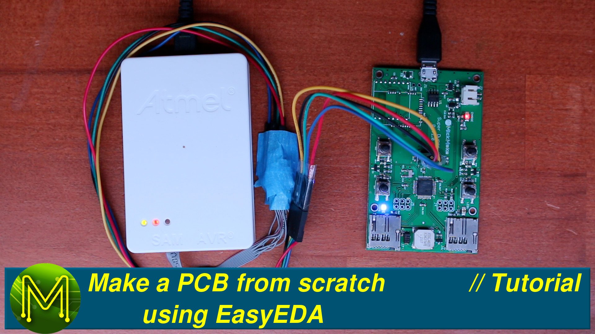
Pick & Place
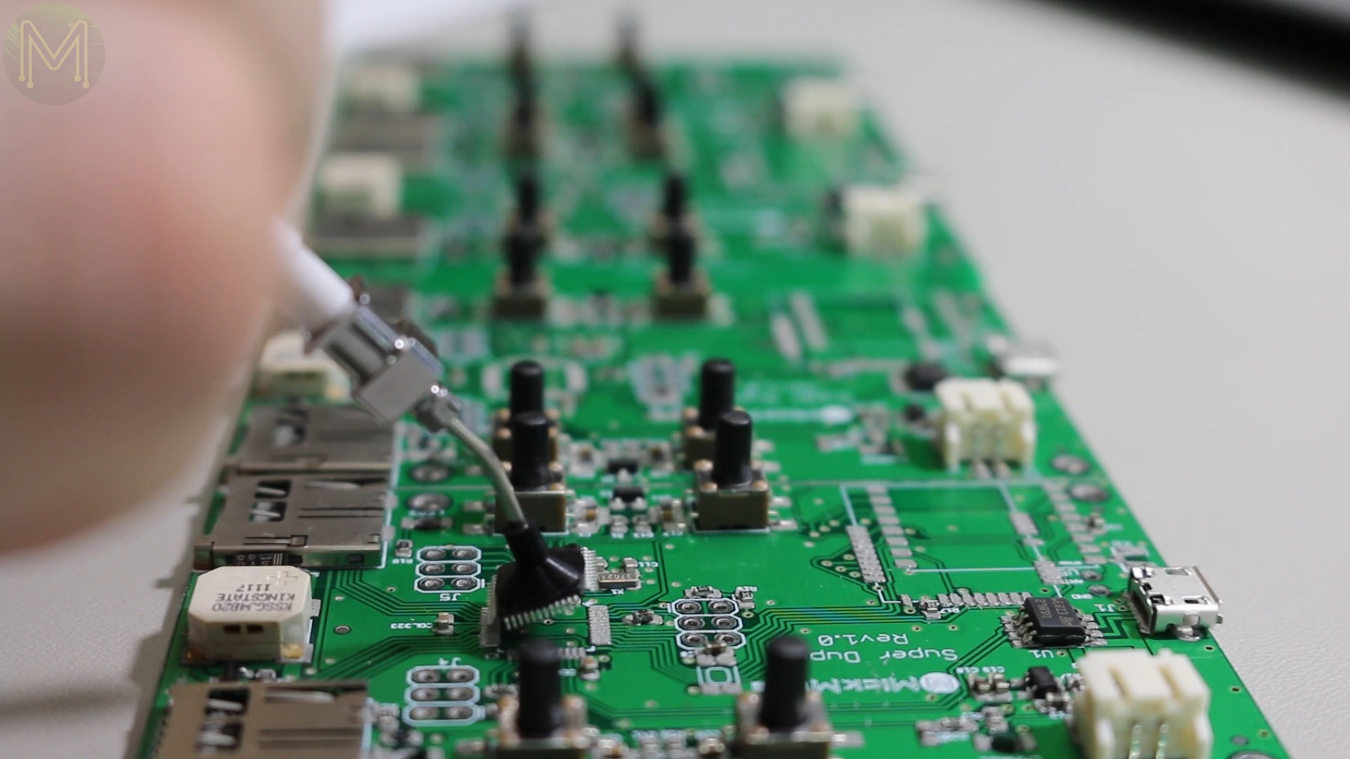
Next is the painstaking bit. Picking and placing components. The larger flatter components are relatively easy.
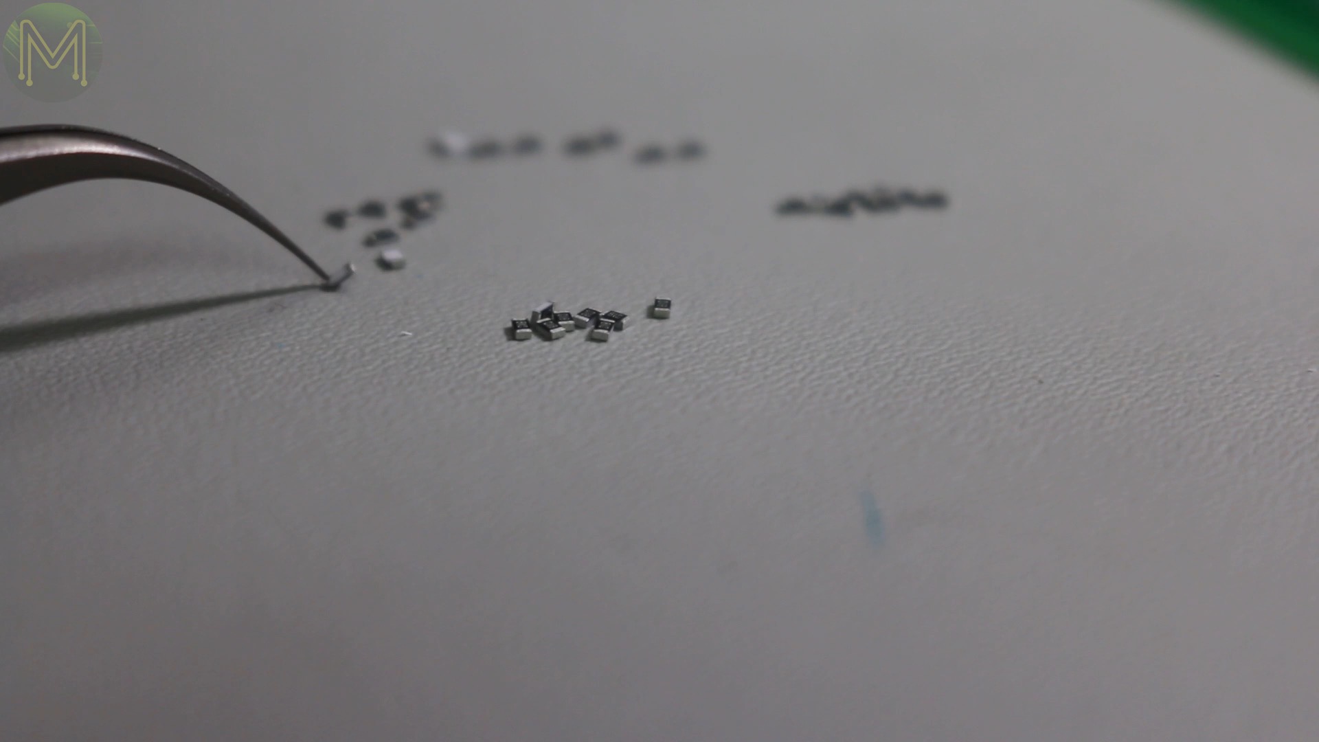
Most of the parts were, thankfully, only 0603s - 0603 refers to the SMD package size. You can work with 0603 fairly easily, but you can also get the smaller 0402 and things get a little crazy when you get down to 0201. There’s even a 008004 standard, which comes in at .2mm by .1mm. See here for some other sizes.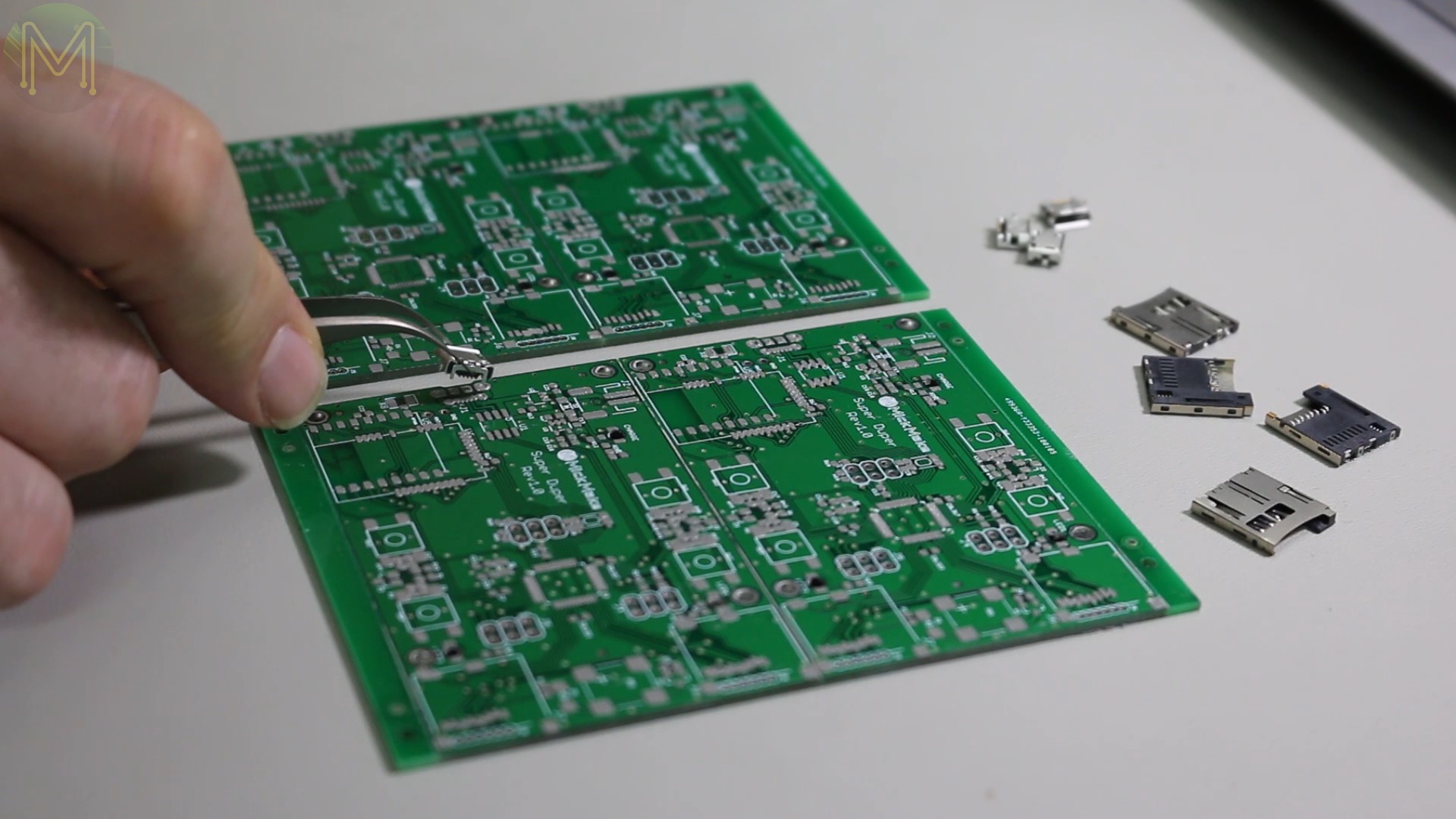
Of course, some parts can be placed in any orientation. Resistors and most capacitors can be placed rotated, upside-down or right-side-up, but the package has really been designed to be placed with the label at the top.
You can flip them around easily like this, but be careful as they can end up flying across the room. And forget ever trying to find even a 603.The amount of solder paste is also important. This is the perfect amount of solder.Whereas in other areas there were large spread-out blobs. This was because I made several passes with the solder screeder.It’s not a huge drama, but it will more than likely increase your time fixing up soldering issues. You’ll discover later how this can affect the final result.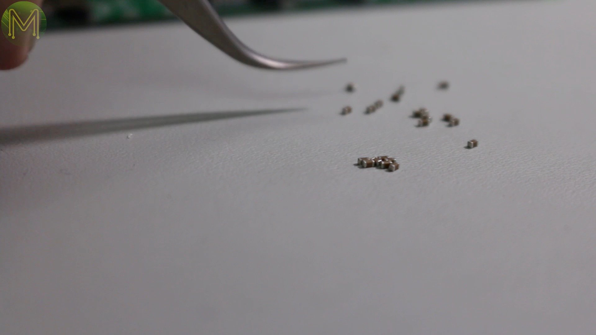
Try to firmly place components down vertically. If you come in from the side, you risk pushing solder paste around. This is often hard to do, especially with a shakey hand.
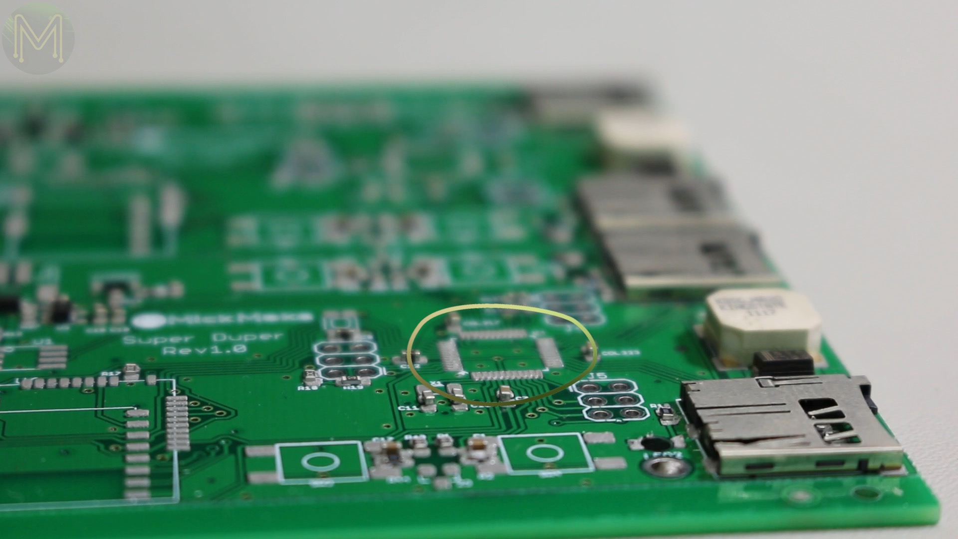
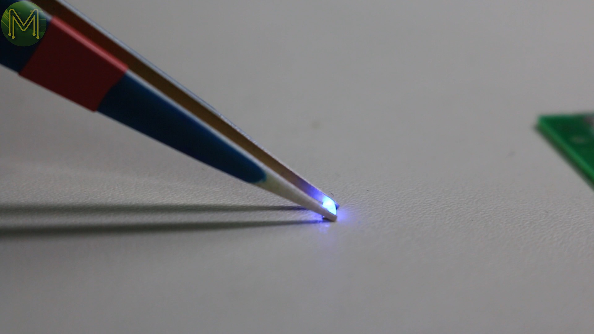
When placing MCUs, it’s pretty important to line up accurately. The more the pins line-up with the pads, the less chance there will be for soldering bridges. Of course these need to be placed with the correct orientation.Along with buzzers, diodes, MosFETs & LEDs. Back in Weekly Roundup #47 we saw the LEDtwee Kickstarter. Essentially a pair of tweezers that tell you the correct LED orientation. They come in handy with this sort of thing.
Reflow soldering
Once you have your PCB fully loaded, it’s off to the cooker. This is called reflow. There’s several different methods, but they all involve heating up the board to around 190 to 210 degrees Celsius.
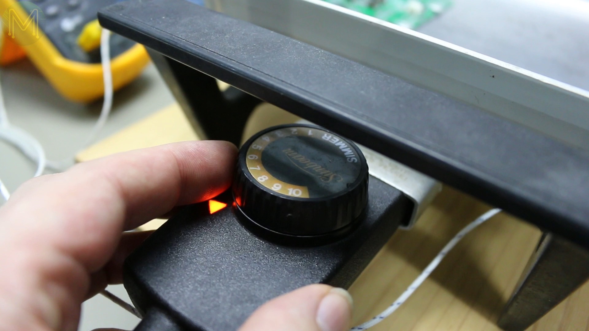
You can use an infrared reflow oven, a ReflowR, commercial Nitrogen reflowers, expensive vapour phase ovens, or just crack out your electric frypan.
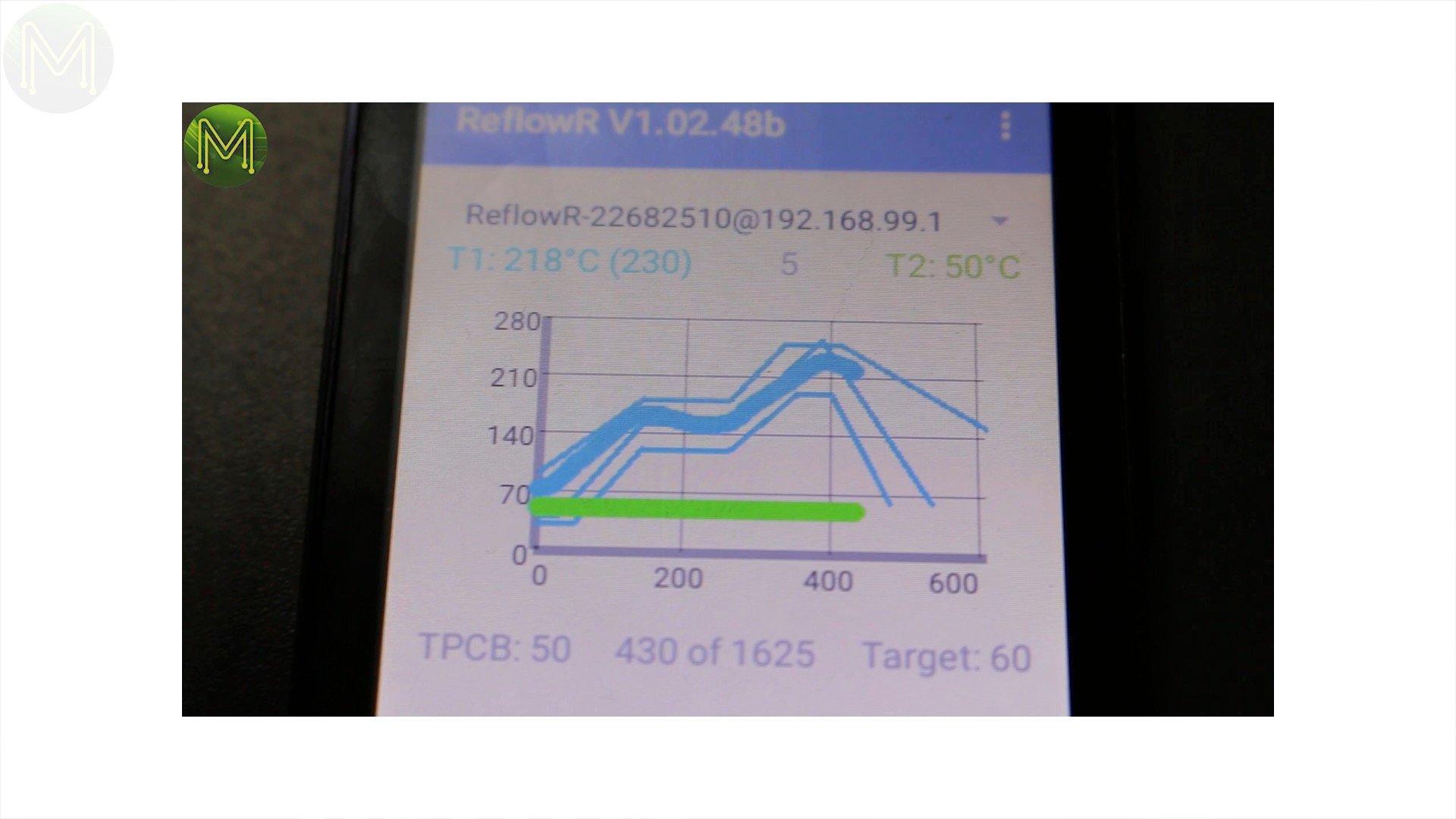
A fry pan with a thermistor attached is good enough for the job. If you saw my ReflowR review video, you’ll have heard me and my mate, Kean, talk about temperature profiles. You can’t just slap heat on to a PCB and expect it to solder. There’s a thing called thermal shock - and it can damage components and cause badly soldered joints.So you need to reflow according to a correct temperature profile. It turns out that the humble fry pan has a mostly accurate temperature profile, just by turning it on until solder melts and then turn off when done.The only downside is that not all the frypan heats up evenly. So using a stick to prod it occasionally helps. Note that as soon as I push down in one area, the PCB makes contact with the frypan and then the solder melts.There’s several things happening here… You’ll see here that too much solder was placed on the PCB, but as the solder starts to melt it is drawn into itself. This is due, thankfully, to surface tension. Without it the whole electronics industry would be very different.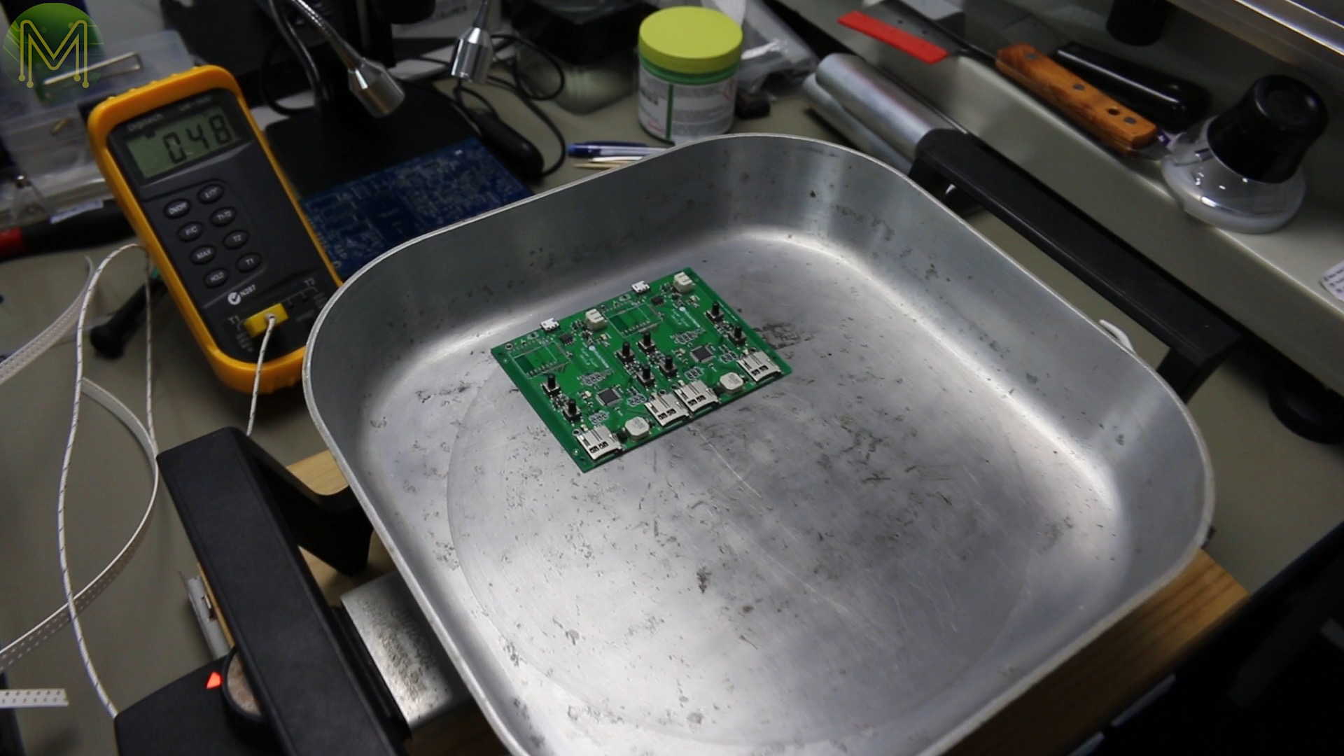

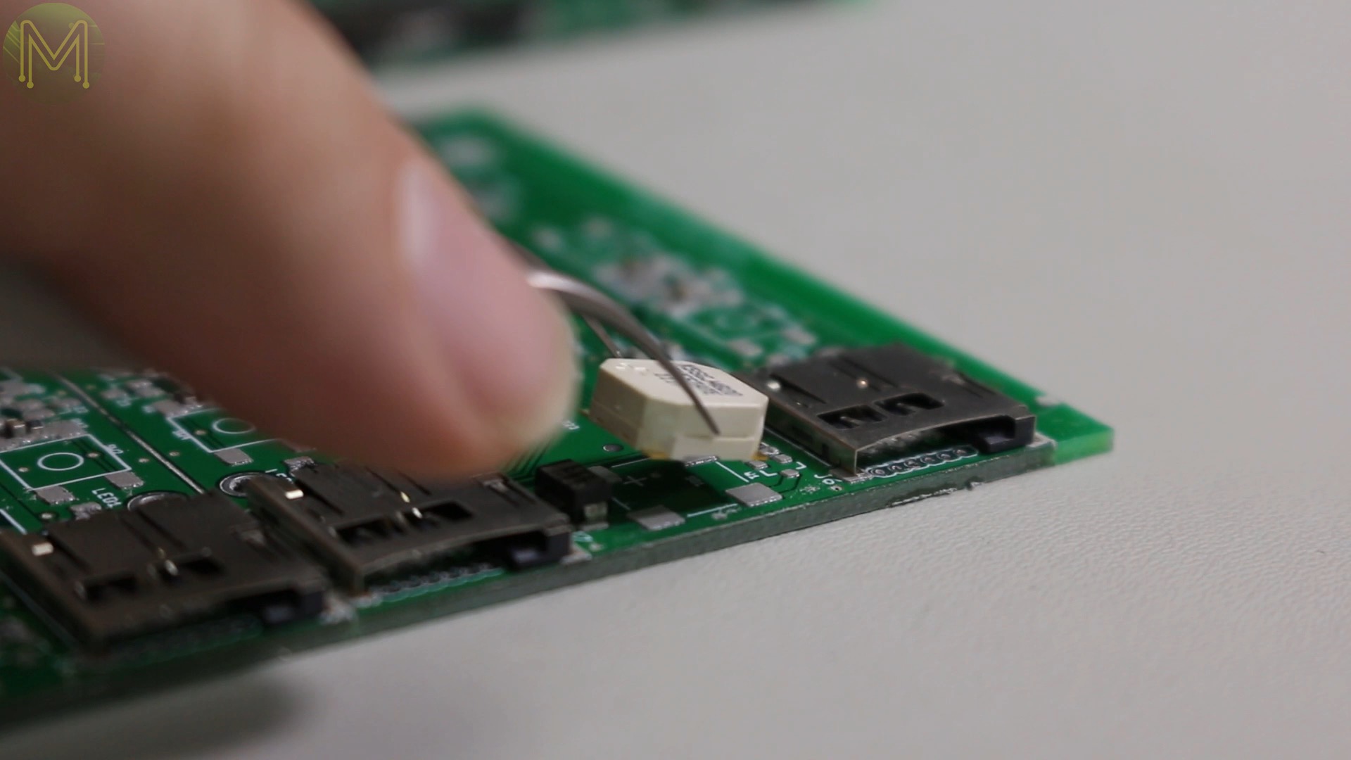
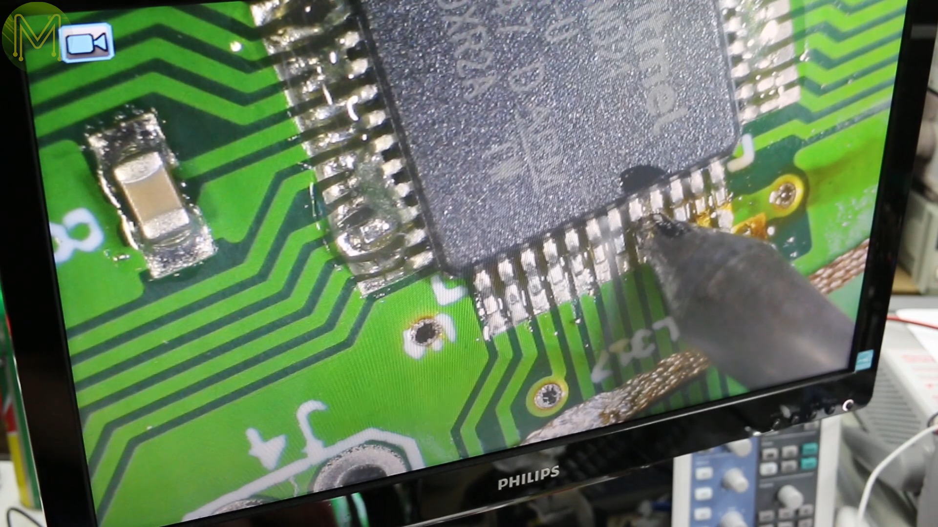
However, sometimes it doesn’t always work like that and incorrectly placed components, (like the MCU), can cause solder bridges.
And some of the larger components didn’t ever reflow, (like the buzzer).
Using a frypan us useful because sometimes components “tombstone”. This is where the surface tension of the solder lifts up a component vertically. Sadly, it never happened for me this time, so I couldn’t show you.
It’s important not to leave it there for too long. So turn it off and keep the PCB in there until it cools down. This is where the thermistor comes in.
Around 50-60 degrees should be good enough.
Fixing up solder bridges is easy enough. A bit of flux and solder wick cleans things up pretty quickly.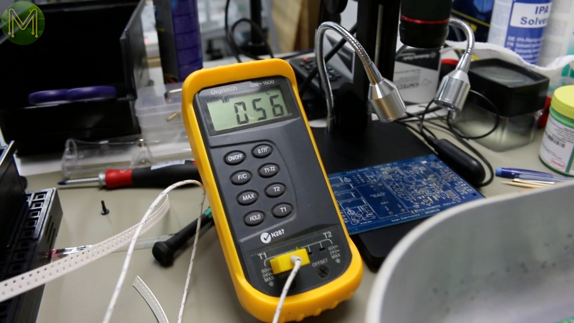

Powering up
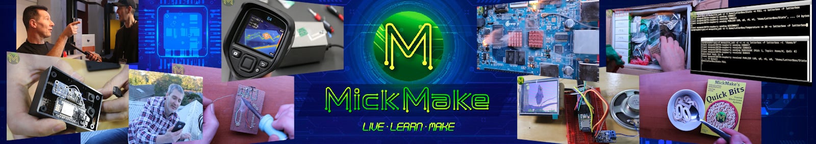
Now that you have your board all soldered up, time to program it. My Super Duper PCB is based on the SAMD21. If you want to know how to flash a boot-loader for the Arduino IDE or just roll your own code from scratch, then check out two of my videos on this that’ll have you up and running in a couple of minutes.

Summary
If you want to make your own boards then I highly recommend using EasyEDA to design it and then ordering the PCBs through their sister company JLCPCB. You can’t go past the offer of getting 10 PCBs for only $2 and at the moment they are offering a $20 shipping discount on your first order.
So, there you have it. You now have everything to make your own PCBs from scratch.